|
|
|
|
|

|
|
← 31211 Bugs Stasi
Covert RF listening device · 375 MHz
- under construction
31211-5 is a radio frequency (RF)
covert listening device (bug),
developed in the late 1960s by PGH Funkmechanik 1 in Freiberg (DDR),
for use by department 26 (German: Abteilung 26) of the repressive
State Security Service (MfS or Stasi)
of the former DDR (East-Germany).
It is a second generation transmitter and works on the
UHF frequencies between 360 and 400 MHz (Band IV).
|
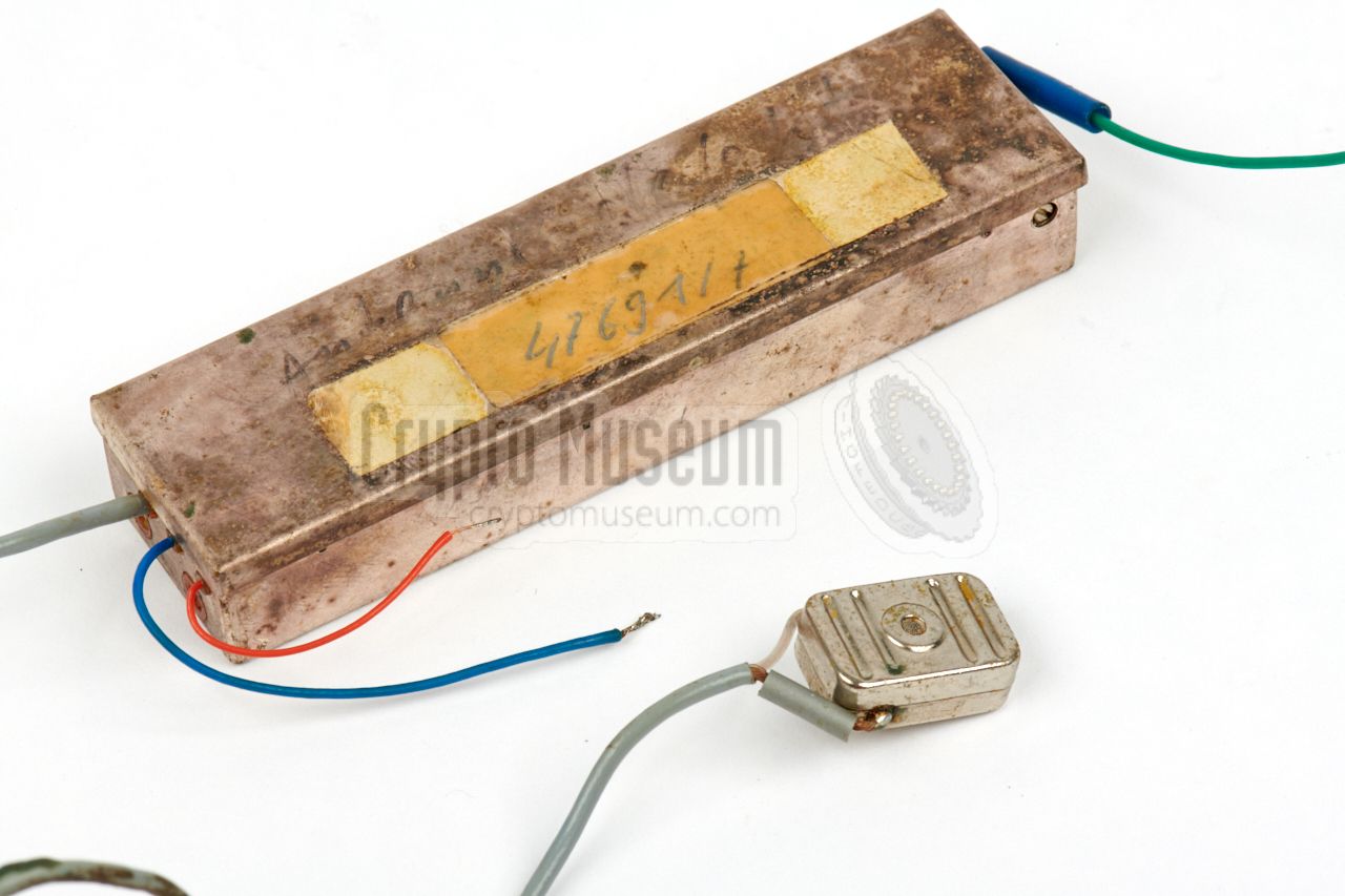
The covert device was intended for overhearing a conversation in a room
and was often used as part of a concealment, for example hidden inside an
object or a piece of furniture. It measures 97 x 26 x 15 mm and
weighs 72 grams, including
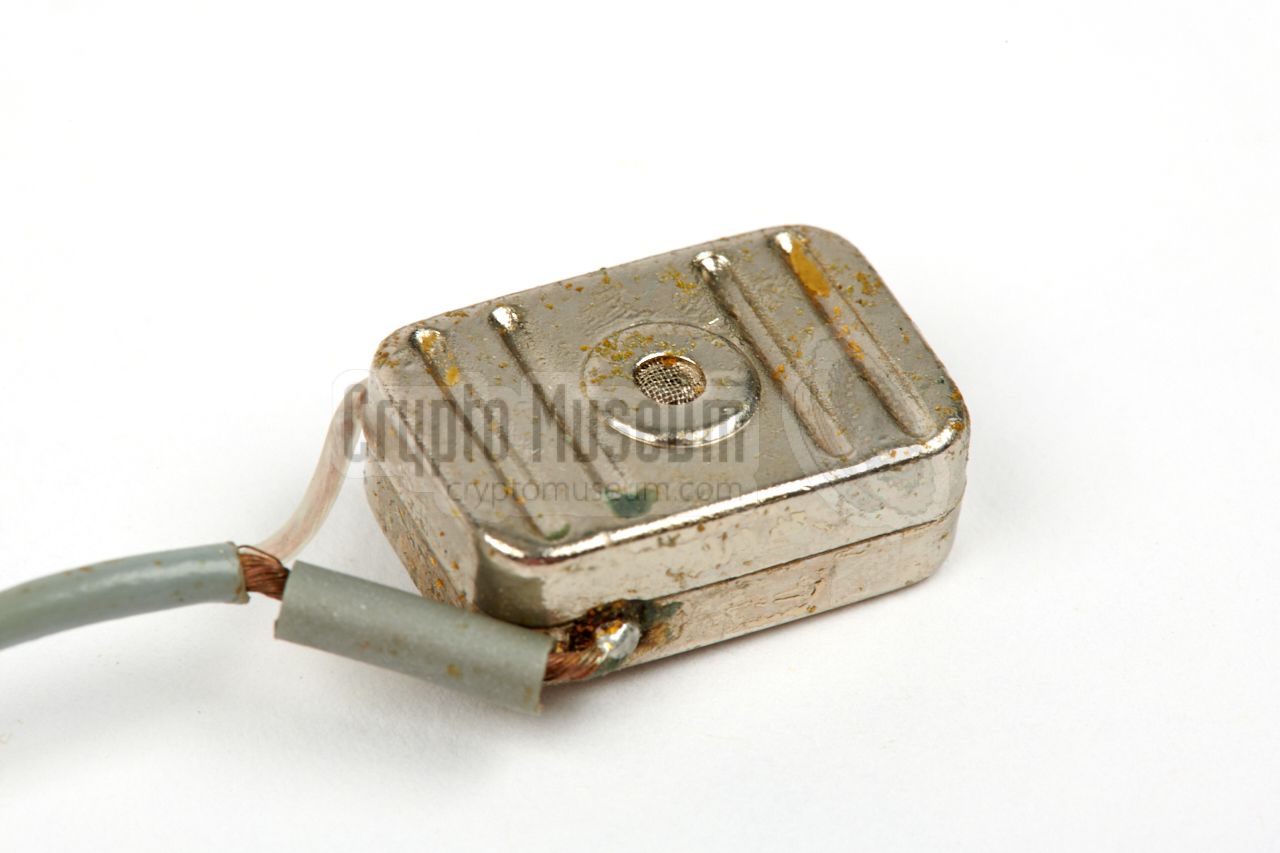
a Sennheiser
MM-21 dynamic microphone.
The image on the right shows a typical 31211-5 with a Sennheiser MM-21
connected to it. At the right is a (green) wire antenna. The red and blue
wires at the left are for connecting a battery or a power supply unit (PSU).
The bug is powered by a 7 to 10V DC source, but performs best at 8.5V.
|
|
|
The device featured here, has been adjusted for a nominal operating
frequency of ~ 375 MHz, which is subject to the supplied voltage, the ambient
temperature and any objects in the vicinity of the transmitter and in particular
its antenna. Despite the fact that it is a two-stage transmitter — it consists
of an oscillator and an RF amplifier — it suffers from the so-called
hand effect, which may cause it to drift as much as 1 MHz at either
side of the nominal frequency of 375 MHz.
The device has a very sensitive built-in audio pre-amplifier
with a high dynamic range, as a result of which any conversations in a room
can be picked up with great ease. The pre-amplifier is built around a
Siemens TAA131
integrated circuit (IC) that had been developed especially
for miniature hearing aids and that had just become available in
countries West of the Iron Curtain
in 1966. 2
|
 |
-
Source: Prof. Schiffel, via Detlev Vreisleben [1].
PGH = Produktions-Genossenschaft des Handwerks.
-
For this reason it is assumed that the 31211-5 was developed no earlier
that the late 1960s.
|
The diagram below gives an overview of the characteristics of the
transmitter. At the front is the wiring for connection of the battery
and an external dynamic microphone.
Also at the front are two small holes
through which the adjustable capacitors of the RF stages can be reached.
At the far end is a 21 cm wire that acts as the antenna. For the best
results, it should be straightened along the longitudinal axis of the device,
in which case the body itself acts as the counterpoise.
At the side of the enclosure, almost at the far end, is a hole behind
which an adjustable capacitor is located. Turning this capacitor 90°
to either side, allows the nominal frequency to be altered by ± 2 MHz.
This should only be done when necessary, as it reduces the performance
somewhat [A].
|
|
The 31211-5 was part of a
family of miniature covert listening devices,
consisting of low-power (short range), medium power (medium range)
and high-power (long range) transmitters, either bare or concealed
inside an object or a piece of furniture.
Most of them were manufactured in the DDR, but some
were obtained from sister agencies in countries like Czechoslovakia and Bulgaria.
|
|
The following variants of the 31211-5 are known:
|
- Standard single-channel version for 2000Ω dynamic microphone (MM-21)
- Dual-channel version (the two channels are mixed)
- With built-in identifier (complete device known as 31221)
- Adapted for external audio masking device (typically a sub-carrier modulator)
|
31211-5 Transmitter (bug) 31211-52 PSU for 31211-5 1 31221 31211-5 with identifier
|
-
Source: MfS, Inventurliste 1987 [4 p.50].
|
The 31211-5 is a two-stage transmitter, which consists of three functional
blocks, as illustrated in the diagram below. At the center is a free running
oscillator that delivers a signal at the desired frequency (375 MHz).
This signal is buffered and amplified in the PA stage at the right.
At the left is a high-gain audio amplifier with a high dynamic range,
that directly modulates the oscillator.
|
Below is the initial circuit diagram of the 31211-5, as found in the
original technical description [A]. Note that this is just an intermediate
design, that does not reflect the actual circuit of the device. The circuit
is built around two RF transistors, of which the first one is the
oscillator (T1). It is modulated directly at its base
by the audio signal from the electret microphone at the far left.
The oscillator has a tuned circuit with a stripline (L1) that is
capacitively coupled to the second stage, which is an RF amplifier
in grounded base configuration (T2).
The antenna is connected directly to a tap on the stripline (L2) of
the tuned circuit of T2. In this design, the (+) terminal of the
battery is connected to the chassis. The circuit is powered by
a voltage between 5.5 and 12V.
|
Below is the circuit diagram of the final design of the device,
as taken down by Crypto Museum in 2018 [5]. This circuit matches the
technical discription in the original documentation [A], but is
significantly diffent from the circuit above.
It is powered by 9V DC and has (-) on the chassis.
This design is also based on two RF transistors, of which T1 is the
oscillator and T2 is the RF amplifier in grounded base configuration.
However, the two stages are transformer-coupled (L1a/L1b) and
a trimmer is present to allow fine tuning by approx. ± 2 MHz.
Furthermore, an AF
amplifier is added at the left. It is based on a very early
TAA131 integrated circuit 1
which was introduced by the West-German company
Siemens
in 1966, especially for use in hearing aids [B].
Note that there are at least four variants
of the audio amplifier section.
The circuit diagram above reflects the basic variant which had a single
input for a 2000Ω microphone. Other variants were available with
dual audio input, a built-in identifier, or an interface to an external
audio masking module. The unpopulated area of the audio board was used
to accomodate these extra features.
|
|
-
This dates the design to the late 1960s.
|
|
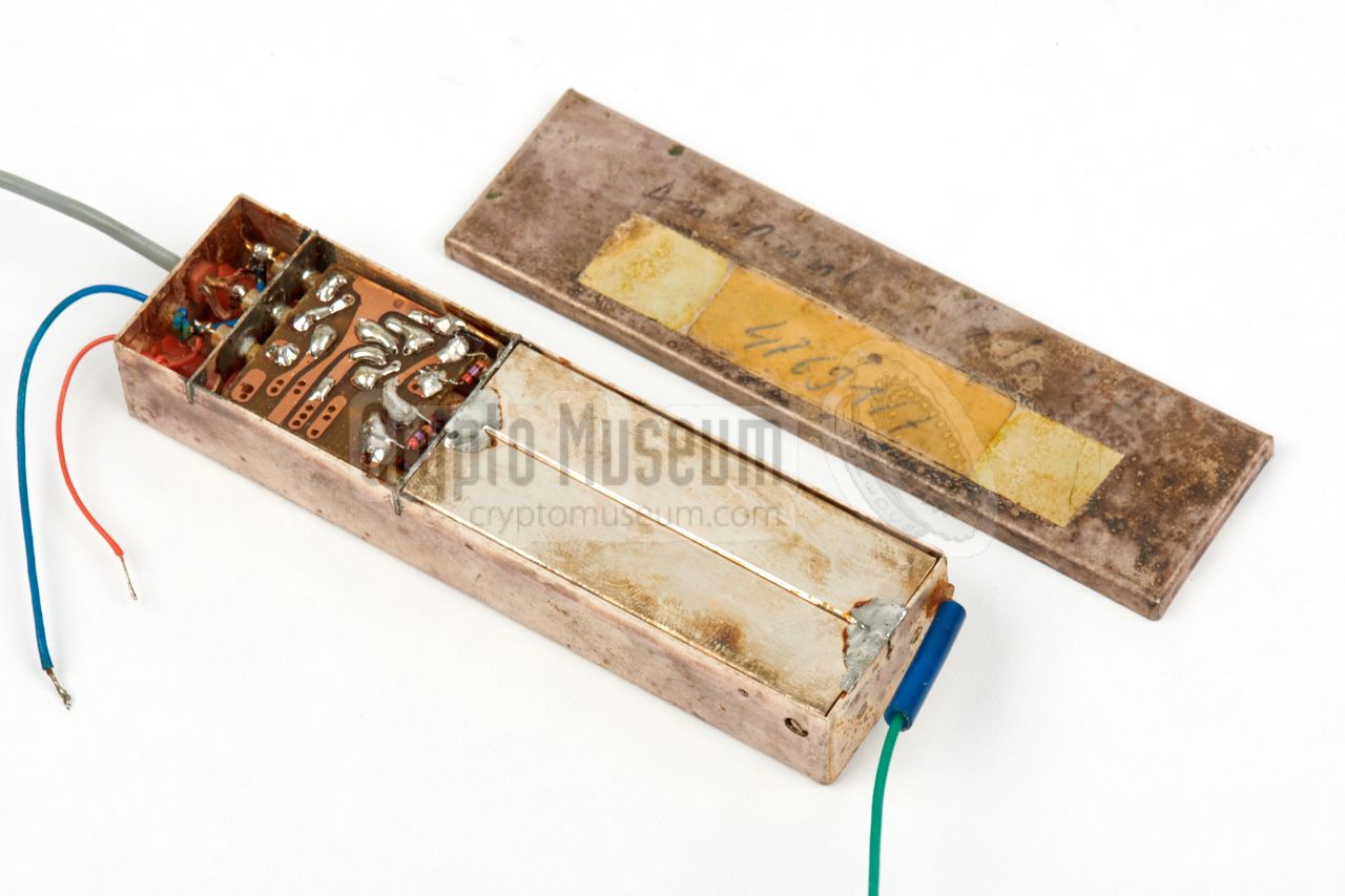
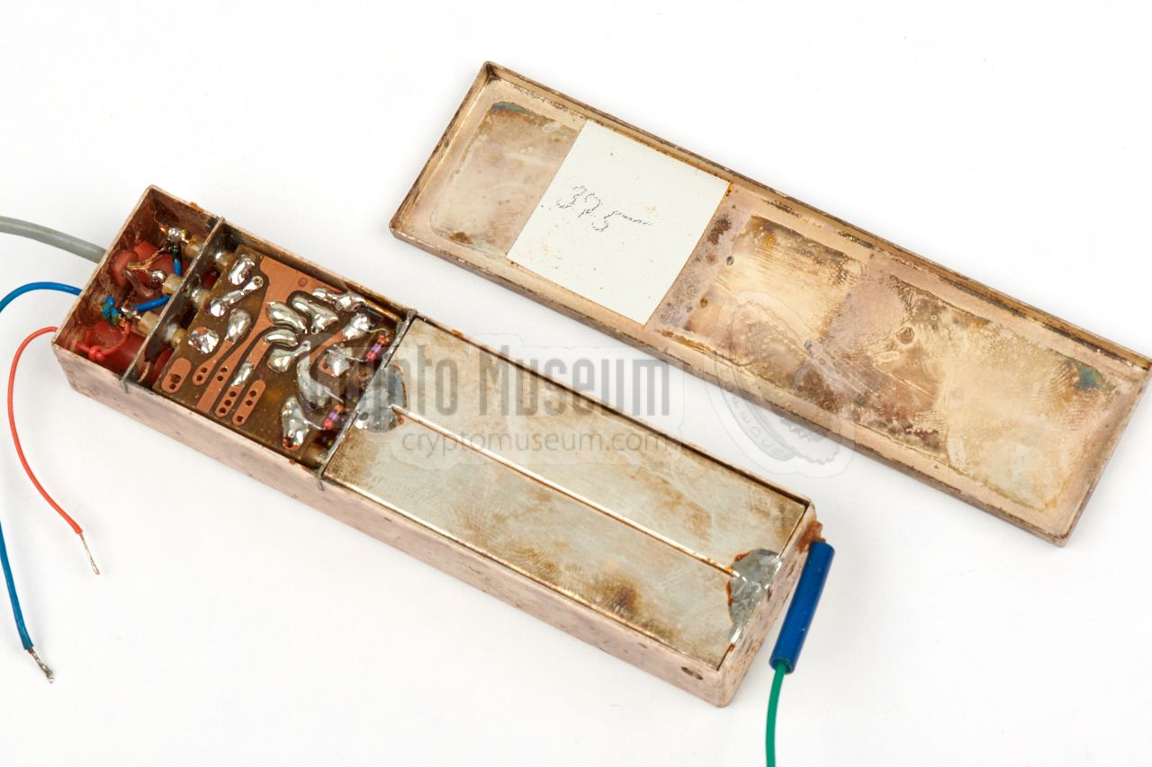
The transmitter is housed in a silver-plated brass enclosure that
measures 97 x 26 x 15 mm. It is closed at one of the large sides
with a silver plated lid that can easily be removed. After lifting
off the lid, the
contents of the bugs are revealed.
The interior is divided into four compartments.
|
The smallest compartment holds the wiring to the external
batteries and the microphone. The wires are connected
to the second compartment via a series of feed-through capacitors.
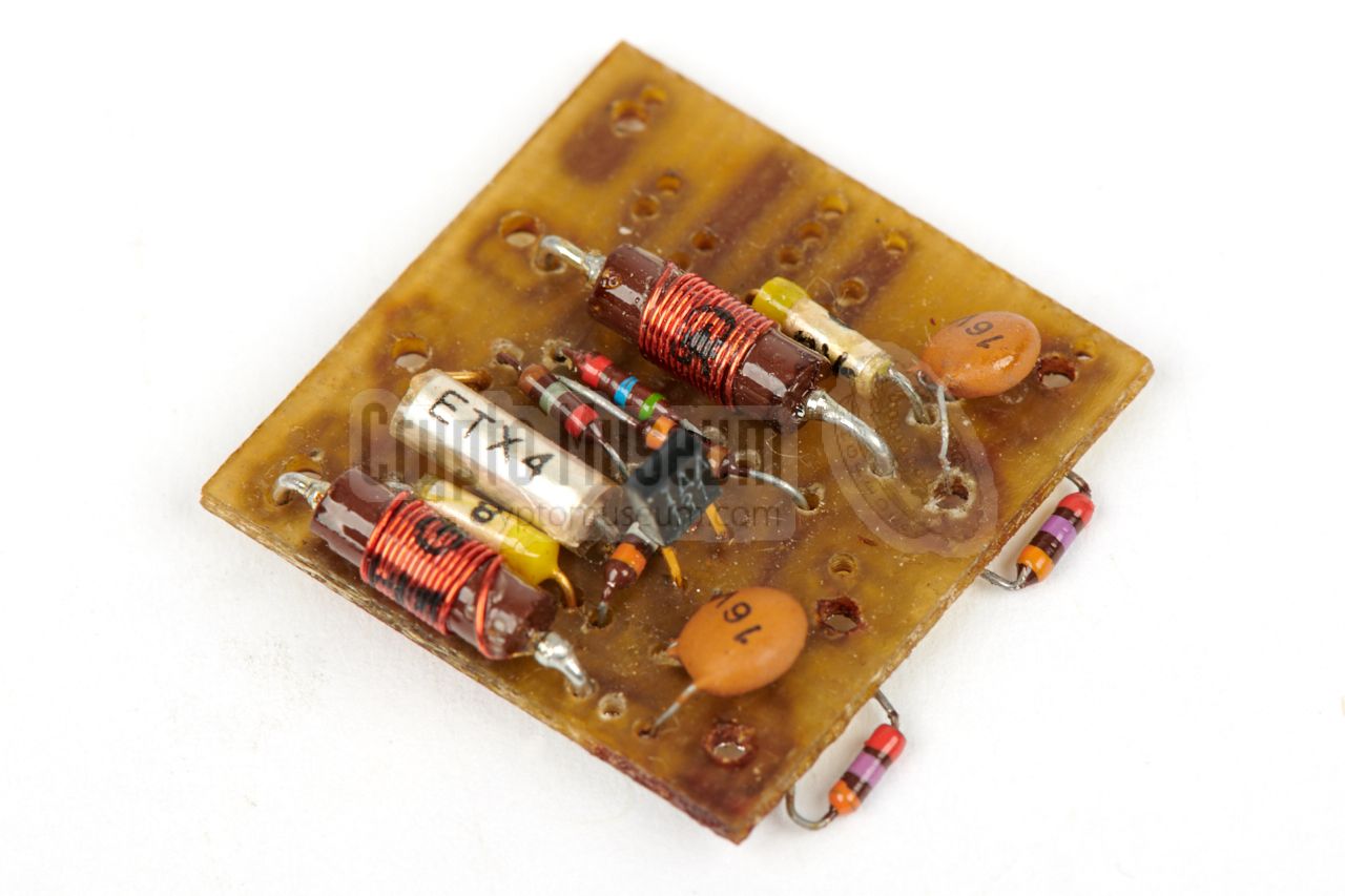
This compartment holds a PCB with the power line filters and
an audio amplifier, which is built around a very early
TAA131 integrated circuit (IC)
from the western manufacturer Siemens.
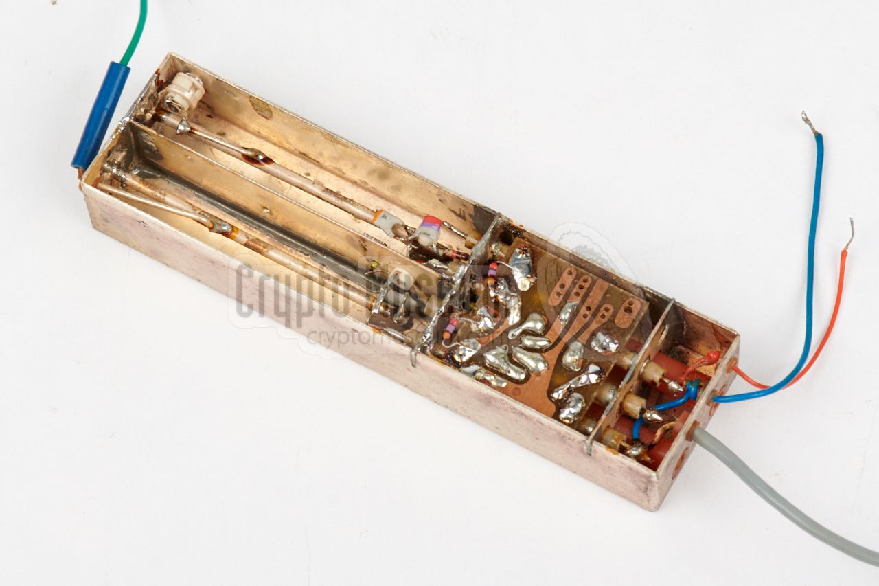
The image on the right shows the amplifier board after
removing it
from the soldered pins of the feed-through capacitors at both sides.
A short wire connects the board to the chassis.
|
|
|
|
The board is partly unpopulated. This space is used for
other variants of the audio modulator.
At the right are two long compartments that hold the RF stages.
They are normally shielded, but for the image at the top of this section,
we have removed them temporarily. The amplifier board is connected to the
RF stages via four feed-through capacitors.
At the solder side of the amplifier board are two 27k resistors
that are directly solderd to the pads of the feed-through capacitors.
|
Two further 4k7 resistors are
soldered directly to two of the feed-through
capacitors below the audio board. Together, these resistors provide the
bias voltage at the base of the RF transistors. The 27k resistors are
probably soldered at the back of the audio board, so that the circuit
can be optimised for a particular supply voltage.
In the given configuration, the best performance was measured
with a power supply of 8.5V DC.
Note the two plastic (red) tubes that run through the amplifier compartment.
They can be used to access the tuning capacitors of the striplines.
|
|
|
|
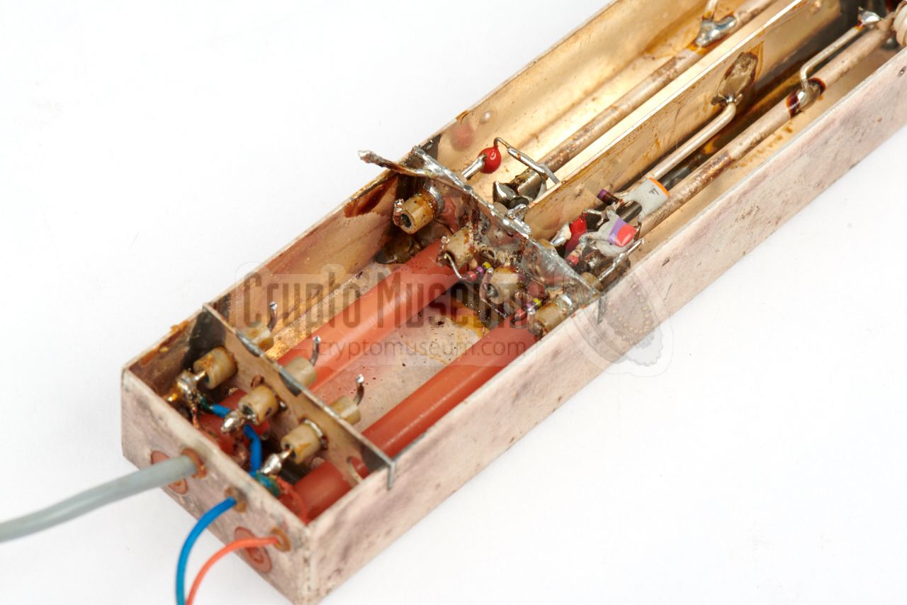
The two long compartments hold the RF stages, each of which is built around
an Japanese NEC 1 2SC289 RF transistor (marked 289), and a tuned circuit
which consists of a stripline (a silver-plated copper wire) with
a tuning capacitor at one end. The other end is soldered to the chassis.
|
The components inside the RF compartments are soldered closely
to the feed-through capacitors from the audio board.
The image on the right gives a good view
of the two white ceramic RF transistors. The one at the rear is the oscillator,
whilst the one at the front is the RF amplifier.
At the left, part of the striplines are visible. At the right are the plastic
red tubes, through which the adjustable capacitors – mounted at the end of the
striplines – can be reached for alignment. The two RF stages are coupled via
a stripline transformer mounted to the separation
wall.
|
|
|
|
About 1/3rd from the ground-end of the oscillator's stripline, is a tap
with a trimmer connected to ground. It allows the nominal frequency of the
transmitter to be shifted by ± 2 MHz, but this should only be
done when it is unavoidable, as it reduces the transmitter's performance.
The antenna is galvanically coupled to the RF amplifier's stripline
at ~ 1/3rd from the ground-end.
|
-
The 2SC289 was manufactured by the Japanese company NEC, but also
by the US company American Microsemiconductor. It is an RF transistor
with an ft of 1.1 GHz. Datasheet wanted
|
Device Covert listening device (bug) Purpose Room overhearing Model 31211-5 Manufacturer PGH Funkmechanik Year 1968 Country DDR User MfS (Stasi), Abteilung 26 Frequency 360 — 398 MHz (typically 375 MHz) Tuning ± 2 MHz (via trimmer) Modulation F3 (FM) Deviation ≥ 25 kHz @ -70dB (1000 Hz, 600Ω) Audio 200 Hz — 60 kHz 1 Input 200Ω (e.g. MM-21) Output 12.5 mW @ 9V (50Ω) Range 400 m Antenna ¼λ (21 cm) Temperature -20 — +50°C Δf temp 40 kHz / °C Δf voltage 0.5 MHz / V Δf env. ± 200 kHz Power 7.2 — 10.5V (9V nominal) Current ≤ 16 mA @ 9V Semiconductors 2 x 2SC289 (RF), 1 x TAA131 (audio), 1 x BC112 (or BC147) 2 Dimensions 97 x 26 x 15 mm (including lid) Weight 70 grams
|
-
This makes the device suitable for subcarrier audio masking modules.
-
Only in certain versions of the modulator.
|
-
Document obtained from BStU [2] and kindly supplied
by Detlev Vreisleben [1].
|
- Detlev Vreisleben, 1211-5 / 31211-5, technical description and instructions
Personal correspondence, September — October 2018.
- Bundesbeauftragte für die Stasi-Unterlagen (BStU) 1
Federal Commissioner for the Stasi-Records.
- Louis Meulstee, 31211-5 (GDR bugs II)
Wireless for the Warrier, Volume 4 Supplement, Chapter 124 v1.00.
Retrieved August 2018.
- MfS, Inventurlisten der operativen Technik
Abteilung 26. Berlin, 10 September 1987. 2
- Paul Reuvers, Circuit diagram of 31211-5 in collection
Crypto Museum, 10 October 2018.
|
-
Full name: Bundesbeauftragte für die Unterlagen des Staatssicherheitsdienstes
der ehemaligen Deutschen Demokratischen Republik
(DDR) —
Federal Commissioner for the Records of the
State Security Service
of the former German Democratic Republic (GDR) —
officially abbreviated to BStU.
-
Document obtained from BStU [2] and kindly supplied
by Detlev Vreisleben [1].
|
|
|
|
Any links shown in red are currently unavailable.
If you like the information on this website, why not make a donation?
© Crypto Museum. Created: Tuesday 09 October 2018. Last changed: Wednesday, 24 December 2025 - 14:27 CET.
|
|

|
|
|


![Circuit diagram as given in the technical documentation [A]](svg/31211-5_circuit_old.svg)
![Actual circuit diagram as taken down by Crypto Museum from the 31211-5 in its collection in October 2018 [5]](svg/31211-5_circuit.svg)


